Applications:
|
|
Features:
|
|
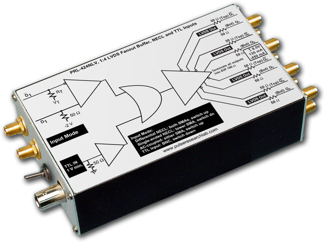
DescriptionThe PRL-424NLV is a 1:4 fanout, complementary output, LVDS line driver. It is intended for converting NECL signals, AC-coupled sine waves, or TTL signals into multiple LVDS signals for driving long lines. The PRL-424LV high speed fanout line driver facilitates testing of high speed digital communications circuits and distribution of satellite signals. The PRL-424NLV has two logically ORed input circuits:
The four pairs of complementary outputs are 50 Ω back-terminated and are designed for driving floating 100 Ω loads, normally the configuration used in LVDS input circuits. The output swing is typically 600 mV with a common mode voltage of 1.2 V. All output connectors are SMA. The PRL-424NLV is supplied with a ±8.5 V/1.8 A AC/DC adapter and housed in a 1.3 x 2.9 x 5-in. extruded aluminum enclosure. Available accessories include voltage distribution modules and brackets for mounting multiple units. (1) A related model, the PRL-424LV, has a "universal differential" input (floating 100 Ω termination) that will accept LVDS, RS-422, NECL and LVPECL, so long as the NECL and LVPECL signals are differential and have internal pull-down resistors. |
 Fig. PRL-424NLV Block Diagram
(0° C ≤ TA ≤ 35° C)*
| SYMBOL | PARAMETER | Min | Typ | Max | UNIT | Comment |
|---|---|---|---|---|---|---|
| RIN | Input Resistance | 49.5 | 50 | 50.5 | Ω | |
| VTT | D Input Termination Voltage (fixed) | -2.2 | -2.0 | -1.8 | V | |
| VT1 | D Input Termination Voltage | -1.17 | -1.30 | -1.43 | V | Switch Down |
| VT2 | D Input Termination Voltage | -2.20 | -2.00 | -1.80 | V | Switch Up |
| VIL | Input Lo Voltage | -1.95 | -1.60 | -1.48 | V | |
| VIH | Input Hi Voltage | -1.13 | -0.90 | -0.81 | V | |
| VOL | Output Low Level | 0.9 | V | |||
| VOH | Output High Level | 1.5 | V | |||
| VIL | Input Lo Voltage | -1.95 | -1.60 | -1.48 | V | |
| IDC1 | DC Input Current, +8.5 V | 130 | 140 | mA | ||
| IDC2 | DC Input Current, -8.5 V | -470 | -480 | mA | ||
| VDC | DC Input Voltage | ±7.5 | ±8.5 | ±12 | V | |
| VAC1 | AC/DC Adapter Input Voltage, 120 | 103 | 115 | 127 | V | |
| VAC1 | AC/DC Adapter Input Voltage, 220 | 206 | 220 | 254 | V | |
| tPLH | Propagation Delay to output ↑ | 2.7 | ns | |||
| tPHL | Propagation Delay to output ↓ | 2.7 | ns | |||
| tr/tf1 | Rise/Fall Times (10%-90%)1 | 500 | 650 | ps | @ 200 MHz | |
| tr/tf2 | Rise/Fall Times (10%-90%)1 | 250 | ps | @ 1.25 GHz | ||
| tSKEW | Skew between any 2 outputs | 200 | 550 | ps | ||
| fMAX1 | Max Clock Frequency, SMA Input2 | 1.25 | 1.35 | GHz | ||
| fMAX2 | Max Clock Frequency, TTL Input | 300 | MHz | |||
| Size | 1.3 x 2.9 x 5.0 | in. | ||||
| Weight | 8 | Oz | ||||
| Shipping Weight | 4 | lbs | ||||