Applications:
|
|
Features:
|
|
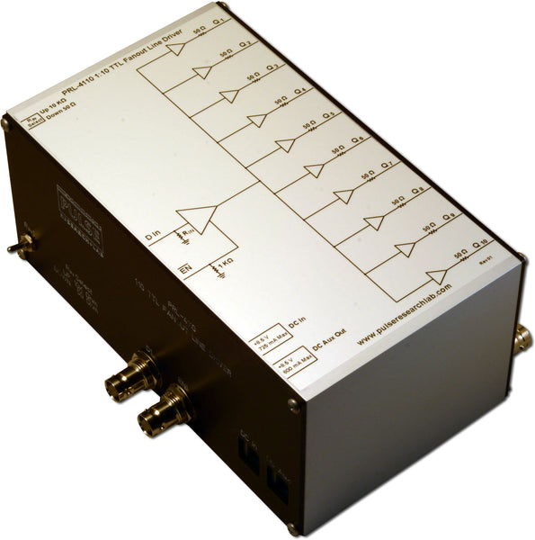
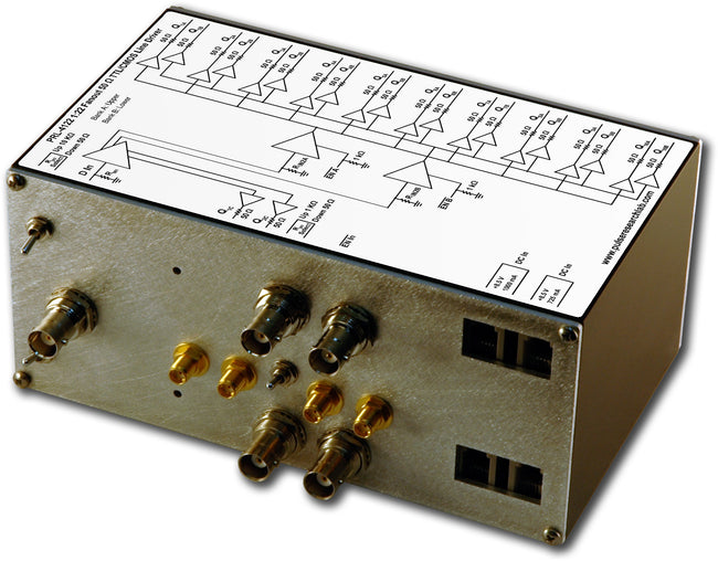
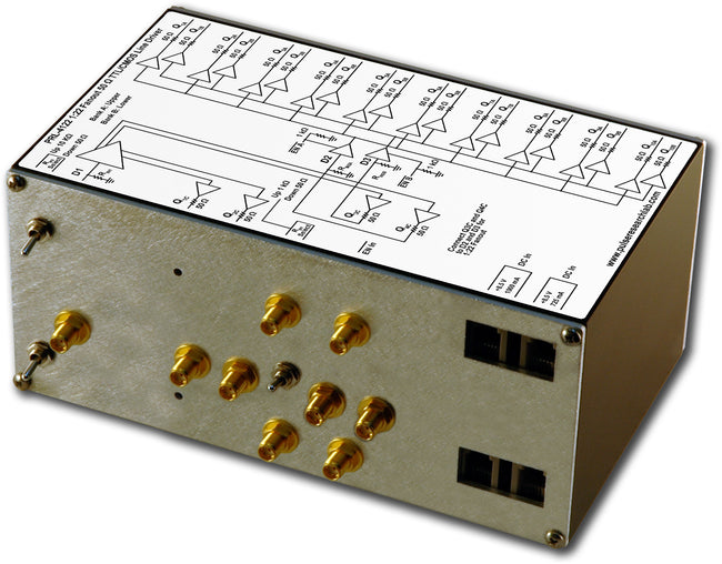
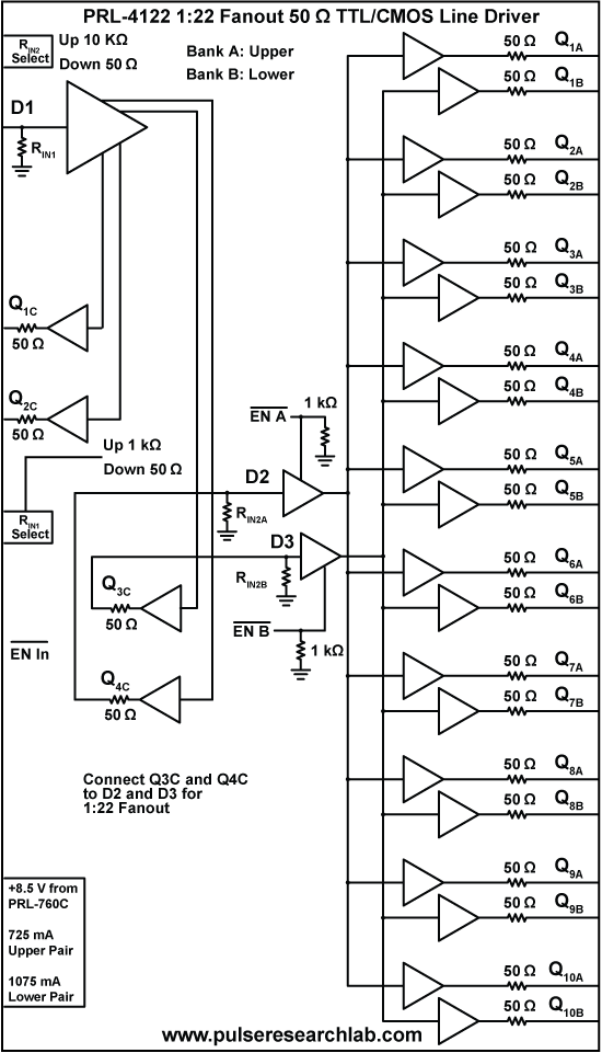
DescriptionThe PRL-4122-BNC is a 1:22 fanout, 50 Ω TTL Line Driver. It is intended for distribution of high-speed clock and logic signals to multiple loads via long lines. The 50 Ω back-terminated outputs can drive long lines with or without 50 Ω load terminations. With 50 Ω load terminations, however, all outputs of the PRL-4122 can drive 100 ft of 50 Ω cables at clock rates greater than 80 MHz. The PRL-4122 is implemented as a 1:4 fanout buffer (equivalent to a PRL-414B module) with two of its outputs externally cabled to the inputs of two 1:10 fanout buffers (each equivalent to a PRL-4110 module). The twenty outputs from the two 1:10 modules are in phase, while the additional two outputs of the 1:4 module are advanced by approximately 10 ns. These auxiliary outputs can be used to drive the inputs of downstream PRL-4110 or PRL-4220 units for additional in-phase outputs. The input resistance of the PRL-4122’s primary input can be selected to be either 50 Ω or 1 kΩ by a switch. The 1 kΩ-input is desirable when interfacing with low power circuits. The 50 Ω back terminated outputs typically deliver 2.5 V into 50 Ω or 5.0 V into Hi-Z loads. All I/Os are DC coupled and have BNC or SMA connectors, except for the auxiliary outputs which are SMA. Each 1:10 fanout bank also has an independent TTL-compatible EN input pulled down via a 1 kΩ resistor. When left open the Enable is active, and the fanout bank will output signals. Each bank can be disabled by driving its EN input high. A block diagram showing the equivalent input and output circuits of the PRL-4122 is shown in Fig. 1. The PRL-4122 is housed in a 3.0 x 6.8 x 4.0-in. extruded aluminum enclosure and is supplied with the PRL-760E, ±8.5 V/±1.8 A AC/DC Adapter. |
|
Related Products: |
(0° C ≤ TA ≤ 35° C)*
| Symbol | Parameter | Min | Typ | Max | Unit | Comments |
|---|---|---|---|---|---|---|
| RIN LO | Input Resistance Low Range | 49.5 | 50 | 50.5 | Ω | |
| RIN HI | Input Resistance High Range | 9.9 | 10.0 | 10.1 | kΩ | |
| RIN EN | Input Resistance, Enable | 1 | kΩ | |||
| ROUT | Output Resistance | 50 | Ω | |||
| VIL | TTL Input Low Level | -0.5 | 0.0 | 0.5 | V | |
| VIH | TTL Input High Level | 2.0 | 2.4 | 5.0 | V | |
| VIL EN | EN Input Low Level | -0.5 | 0.0 | 0.5 | V | |
| VIH EN | EN Input High Level | 2.0 | 2.4 | 5.0 | V | Drive EN High to disable output |
| VOL | TTL Output Low Level | 0.0 | 0.25 | 0.5 | V | RL=50 Ω |
| VOH1 | TTL Output High Level | 2.2 | 2.5 | V | RL=50 Ω @ DC | |
| VOH2 | TTL Output High Level | 4.4 | 5.0 | V | RL=1 MΩ @ DC | |
| IDC1 | DC Input Current | 1220 | mA | F =50 MHz sq. wave(1) | ||
| IDC2 | DC Input Current | 1510 | mA | F ≤ 100 MHz | ||
| IDC3 | DC Input Current | 1800 | mA | F =125 MHz | ||
| VDC | DC Input Voltages | 7.75 | 8.50 | 12.00 | V | |
| VAC | AC/DC Adapter Input Voltage | 103 | 115 | 127 | V | |
| TPLH1 | Propagation Delay to output ↑ | 19 | 22 | ns | For 1:20 primary outputs | |
| TPHL1 | Propagation Delay to output ↓ | 19 | 22 | ns | For 1:20 primary outputs | |
| TPLH2 | Propagation Delay to output ↑ | 10 | 12 | ns | For 2 auxiliary outputs | |
| TPHL2 | Propagation Delay to output ↓ | 8 | 12 | ns | For 2 auxiliary outputs | |
| tr | Rise Time (10%-90%) | 1.8 | 2.5 | ns | ||
| tf | Fall Times (10%-90%) | 1.5 | 2.5 | ns | ||
| TSKEW1 | Skew between any 2 outputs | 500 | 900 | ps | Within one 1:10 bank | |
| TSKEW2 | Skew between any 2 outputs | 1200 | 1600 | ps | Any two primary outputs | |
| FMAX1 | Max. Clock Frequency(2) | 100 | 125 | MHz | RG58C/U, cable length =3 ft | |
| FMAX2 | Max. Clock Frequency(3) | 80 | RG58C/U, cable length = 100 ft | |||
| PWMIN1 | Minimum Pulse Width | 4 | ns | ↑ Input | ||
| PWMIN2 | Minimum Pulse Width | 6 | ns | ↓ Input | ||
| Size | 3.0 x 6.8 x 4.0 | in | ||||
| Weight | 2 | lb | Excluding AC adapter | |||
| Shipping Weight | 6 | lb | Including AC adapter | |||