Applications:
|
|
Features:
|
|
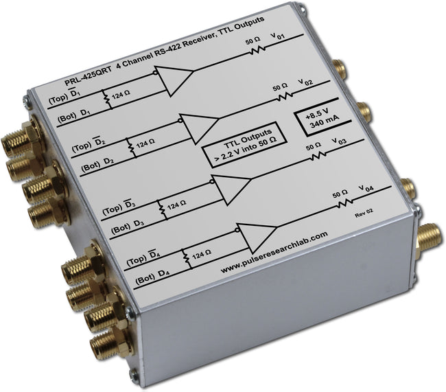
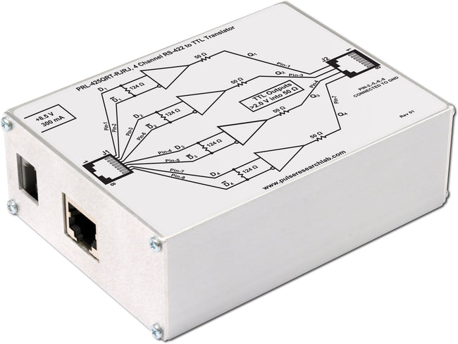
DescriptionThe PRL-425QRT is a four channel, differential input receiver with single-ended 50 Ω TTL output line drivers. It is intended for converting differential signals transmitted through long lines into single-ended TTL outputs. The floating 124 Ω inputs are designed to be compatible with RS-422 input signals. They can also accept source-biased LVPECL inputs. The 50 Ω back-terminated TTL output line drivers can drive long lines with or without terminations, and they are designed specifically for use with high speed data communication applications. Fig. 1 shows the standard RS-422 input configuration. A functional block diagram of this device is shown in Fig. 2. A feature of the RS422 receiver chip in the PRL-425QRT is a “fail safe” state that sets the output logic Hi (TTL True) if the inputs are at the same voltage, which occurs if the inputs are left to float open or if they are shorted to GND. If this is undesired in your application, please consider the PRL-425T, 2 Ch. Universal Differential Receiver with TTL Outputs. Each PRL-425QRT is supplied with a 8.5 V/1.7 A AC/DC Adapter, but it can also operate from a single positive power supply in the range of 7.5 V to 12 V. The PRL-425QRT-SMA has SMA I/Os and is housed in a 1.3 x 2.9 x 2.9-in. extruded aluminum enclosure, while the PRL-425QRT-RJRJ has RJ45 I/Os and a length of 3.9-in. The PRL-425QRT-RJRJ allows the replacement of up to 12 coax cables by 2 double-shielded Cat7/Cat8 network cables to reduce cabling and complexity in high-density applications. While Cat7/Cat8 cabling was designed to carry differential signaling, such as RS422, the shielded twisted pairs have a single-ended impedance of ~54 Ohms when one wire is grounded, and they can carry single-ended TTL signals at up to 100 MHz, as shown in our impedance study. A future version, PRL-425QRT-RJS, with RJ45 inputs and SMA outputs, is planned, but with no guarantee of an availability date. Available accessories include TTL Fanout modules, voltage distribution modules, brackets for mounting multiple units, and a rackmount enclosure kit for rapid system integration. |


SPECIFICATIONS (0° C ≤ TA ≤ 35° C)*
| Symbol | Parameter | Min | Typ | Max | Unit | Comments |
|---|---|---|---|---|---|---|
| RIND | Differential Input Resistance | 124 | Ω | |||
| RINC | Common Mode Input Resistance | 5K | Ω | |||
| IDC1 | DC Input Current @ 50 MHz | 265 | 280 | mA | ||
| IDC2 | DC Input Current @ 85 MHz | 340 | 360 | mA | ||
| VID | Differential Input(1) | V | ||||
| VIA | Single ended input(1) | V | ||||
| VCM | Common Mode Input(1) | -2.5 | 5.0 | V | ||
| VDC | DC Input Voltage | 7.5 | 8.5 | 12.0 | V | |
| VAC | AC/DC Adapter Input Voltage | 103 | 115 | 127 | V | |
| VOHNL | Output Hi Level, No Load | 4.4 | 5.0 | V | RL=1 MΩ @ DC | |
| VOHFL | Output Hi Level, Full load | 2.2 | 2.5 | V | RL=50 Ω @ DC | |
| VOLNL | Output Lo Level, No Load | -0.1 | 0.0 | 0.4 | V | RL=1 MΩ @ DC |
| VOLFL | Output Lo Level, Full Load | -0.05 | 0.00 | 0.20 | V | RL=50 Ω @ DC |
| TPLH | Propagation Delay to output ↑ | 2.2 | ns | |||
| TPHL | Propagation Delay to output ↓ | 2.2 | ns | |||
| tr | Rise Time (10%-90%) | 1.8 | 2.5 | ns | ||
| tf | Fall Time (10%-90%) | 1.8 | 2.5 | ns | ||
| TSKEW | Skew between any 2 outputs | 250 | 600 | ps | ||
| FMAX1 | Max. Clock Frequency(2) | 70 | 75 | MHz | ||
| DTY | Positive Duty Cycle @ 50 MHz | 55 | % | ↑ Input | ||
| Size | 1.3 x 2.9 x 2.9 | in | -SMA version | |||
| Size | 1.3 x 2.9 x 3.9 | in | -RJRJ version | |||
| Weight, excluding AC adapter | 5 | Oz | ||||
| Shipping weight, Including AC adapter | 4 | lb | ||||
(1): See Fig. 1

While we believe these models to be accurate, no representations are made as to accuracy or suitability for any application:
PRL-425QRT-SMA: