

Applications:
|
|
Features:
|
|
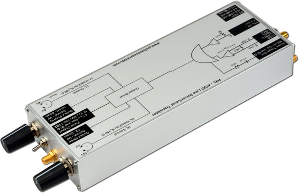
DescriptionThe PRL-470D is a high speed 50 Ω Line Driver/Level Translator with independently variable output Hi and Lo levels. It has a TTL and a Universal Differential Input. The TTL input has a 50 Ω to ground termination, and Universal Differential Input has a floating 100 Ω termination. The floating differential input accepts LVDS, LVPECL, NECL, RS 422, or any 100 mVPP minimum differential signal within the window of -2 V to +3 V. The TTL and Universal Differential Input are logically ORed; therefore a Hi level applied to either input can be used as a gate signal. The PRL-470D is an improved version of the earlier Model PRL-470B. The connectors for the universal differential input are SMA, and the connector for the TTL input is BNC. The output connector is SMA. The trigger output generates > 400 mV into 50 Ω or > 800 mV into high impedance, and is back terminated into an AC coupled 50 Ω source. The self-contained 1.3 x 2.9 x 8.1-in module is supplied with a 8.5 V/+17 V AC/DC adapter. |

SPECIFICATIONS (0° C ≤ TA ≤ 35° C)*
| Symbol | Parameter | Min | Typ | Max | Unit | Comments |
|---|---|---|---|---|---|---|
| RIN_TTL | Input Resistance, TTL | 49.5 | 50.0 | 50.5 | Ω | |
| RIN_DIFF | Input Resistance, Universal Differential | 100 | Ω | |||
| VIL_TTL | TTL input Low Level | -0.5 | 0.0 | 0.5 | V | |
| VIH_TTL | TTL input High Level | 0.8 | 0.85 | 5.0 | V | |
| VIL_DIFF | Differential Input, Low Level | -2 | 3 | V | ||
| VIH_DIFF | Differential Input, High Level | -2 | 3 | V | ||
| VINPP | Differential Input, Peak to Peak | -2 | ±0.1 | 3 | V | |
| VOL1 | Output Low Level, RL = 50 Ω | -3 | 0 | V | ||
| VOL2 | Output Low Level, RL = 1 MΩ | -6 | 0 | V | ||
| VOH1 | Output High Level, RL = 50 Ω | 0 | 5 | V | ||
| VOH2 | Output High Level, RL = 1 MΩ | 0 | 10 | V | ||
| VPP1 | Output Voltage Swing, RL = 50 Ω | 0.8 | 8 | V | ||
| VPP2 | Output Voltage Swing, RL = 1 MΩ | 1.6 | 16 | V | ||
| IDC1 | Max. DC Input Current, +8.5 V | +380 | +390 | mA | ||
| IDC2 | Max. DC Input Current, -8.5 V | -465 | -465 | mA | ||
| IDC3 | Max. DC Input Current, +17 V | +140 | +180 | mA | ||
| VDC1 | DC Input Voltage, +8.5 V | +7.5 | +8.5 | +12 | V | |
| VDC2 | DC Input Voltage, -8.5 V | -12 | -8.5 | -7.5 | V | |
| VDC3 | DC Input Voltage, +17 V | +15 | +17.5 | +20 | V | |
| VAC1 | AC/DC Adapter Input Voltage | 108 | 120 | 132 | V | 120 VAC |
| VAC2 | AC/DC Adapter Input Voltage | 216 | 240 | 234 | V | 220 VAC |
| tPLH/tPHL_VO | Prop. Delay to Output ↑/↓ | 5.5 | 7.5 | ns | VOL = 0 V, VOH = 5 V | |
| tr1 | Output Rise Time (10%-90%) | 850 | 900 | ps | VOL = 0 V, VOH = 5 V | |
| tf1 | Output Fall Time (10%-90%) | 1100 | 1600 | ps | VOL = 0 V, VOH = 5 V | |
| tr2 | Output Rise Time (10%-90%) | 625 | 800 | ps | VOL = 0 V, VOH = 3.5 V | |
| tf2 | Output Fall Time (10%-90%) | 950 | 1100 | ps | VOL = 0 V, VOH = 3.5 V | |
| tr3 | Output Rise Time (10%-90%) | 750 | 800 | ps | VOL = -2.5 V, VOH = 2.5 V | |
| tf3 | Output Fall Time (10%-90%) | 1200 | 1300 | ps | VOL = -2.5 V, VOH = 2.5 V | |
| tr4 | Output Rise Time (10%-90%) | 950 | 1000 | ps | VOL = -3 V, VOH = 5 V | |
| tf4 | Output Fall Time (10%-90%) | 1400 | 1600 | ps | VOL = -3 V, VOH = 5 V | |
| tSKEW | Skew between VO↑ and VO↓ | 100 | 300** | ps | VOL = 0 V, VOH = 5 V, f = 50 MHz, PW = 5 ns |
|
| fmax1 | Maximum Clock Frequency | 225 | 250 | MHz | VOL = 0 V, VOH = 5 V | |
| fmax2 | Maximum Clock Frequency | 250 | 300 | MHz | VOL = 0 V, VOH = 3.5 V | |
| fmax3 | Maximum Clock Frequency | 250 | 300 | MHz | VOL = -2.5 V, VOH = 2.5 V | |
| fmax4 | Max. Input Clock Frequency | 500 | 600 | MHz | Square Wave Mode | |
| PWMIN | Minimum Output Pulse Width | 2.0 | 2.5 | ns | VPP = 5 V | |
| ΔPW | Output PW change, VO↑ to VO↓ | 200 | 400* | ps | VO = 0 to 5 V, PW = 5 ns | |
| VO_Trig | Trigger Output | 1.0 | 1.2 | V | RL = 50 Ω, f ≤ 250 MHz | |
| Size | 1.3 x 2.9 x 8.1 | in. | ||||
| Weight | 13 | Oz | ||||
** Skew and ∆PW may vary with different output level, frequency and pulse width settings.


