Applications:
|
|
Features:
|
|
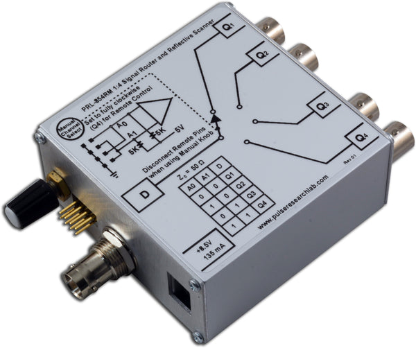
DescriptionThe PRL-257-2 is an AC-coupled input, manually programmable, two phase frequency divider with two sets of complementary NECL outputs. It is capable of running at input frequencies in excess of 6.6 GHz. It has a common divide-by-2 pre-scalar front end followed by two banks of independent manually programmable dividers, Φ1 and Φ2. The f/2 pre-scalar output is further divided by 1, 2, 4, or 8 for the Φ1 bank via D0 and D1 of a two-bit DIP switch, providing a maximum ratio of 16. It is divided by 2, 4, 8 or 16 for the Φ2 bank via D2 and D3 of a second two-bit DIP switch, providing a maximum ratio of 32. All outputs are synchronous with the input frequency and are square waves (50% duty cycle) suitable for driving long lines terminated into 50 Ω/-2 V or AC-coupled 50 Ω loads. The PRL-257-2 is ideal for applications where a high frequency divider or pre-scalar is needed for triggering or down-sampling. The two phases of output enable applications requiring two different ratios from a common reference frequency, and the 1:2 fanout feature enables system synchronization and monitoring/triggering applications from a single reference clock source. Applications for the PRL-257-2 include data acquisition, test, measurement, R&D, and system integration. The unit includes an AC adapter for ready-to-use convenience on the bench or in a system. All I/O connectors are SMA. The extruded aluminum housing is suitable for mounting with the optional brackets. |

Fig. 2: PRL-257-2 Block Diagram
SPECIFICATIONS (0° C ≤ TA ≤ 35° C)*
| Symbol | Parameter | PRL-257-2 | Unit | Comments | ||
|---|---|---|---|---|---|---|
| Min | Typ | Max | ||||
| RIN | Input Resistance | 50 | Ω | AC Coupled | ||
| CC | Coupling Capacitor | 0.08 | 0.10 | 0.12 | µf | Input TC=50 µs |
| IDC1 | DC Input Current, +8.5 V | +80 | +100 | |||
| IDC2 | DC Input Current, -8.5 V | -285 | -300 | mA | ||
| VDC | DC Input Voltage | ±7.5 | ±8.5 | ±12 | V | |
| VAC | AC/DC Adapter Input Voltage | 103 | 115 | 127 | V | |
| VINmin | Minimum p-p Input Amplitude | 500 350 100 |
400 250 50 |
mV mV mV |
Sine Wave@ FMIN In I Square Wave, tr < 2 ns Square Wave, tr < 500 ps |
|
| VINmax | Maximum p-p Input Amplitude | 2.00 | 1.25 | V | Sine or Square Wave | |
| VOH | Output Hi Voltage @ 100 MHz | -1.13 | -0.90 | -0.81 | V | Output terminated to 50 Ω/-2 V |
| VOL | Output Lo Voltage @ 100 MHz | -1.95 | -1.60 | -1.48 | V | Output terminated to 50 Ω/-2 V |
| tPLH | Propagation Delay to Φ1 output ↑ | 2500 | ps | |||
| tPHL | Propagation Delay to Φ1 output ↓ | 2500 | ps | |||
| tr/tf | Rise/Fall Times (20%-80%) | 200 | 250 | ps | Note (1) | |
| tSKEW1 | Skew ↔ Φ1 or Φ2 outputs | 40 | 120 | ps | ||
| tSKEW2 | Skew ↔ Φ1 and Φ2 outputs | 40 | 120 | ps | D0/D1=10, D2/D3=00 | |
| Jitter, p-p | 5 | 10 | ps | Note (2) | ||
| FMIN In I | Minimum Input frequency | 120 | 100 | MHz | Sine wave input | |
| FMIN In II | Minimum Input frequency | 150 | 100 | KHz | Square wave input, tr < 2 ns | |
| FMAX In I | Maximum Input frequency | 6.0 | 6.6 | GHz | ||
| FMAX Out1 | Maximum Output frequency, Φ1 | 3.00 | 3.30 | GHz | Φ1 outputs | |
| FMAX Out2 | Maximum Output frequency, Φ2 | 1.50 | 1.65 | GHz | Φ2 outputs | |
| Size | 1.3 x 2.9 x 2.9 | in. | ||||
| Weight, excl. AC adapter | 10 | Oz. | ||||
| Shipping weight, incl. AC adapter | 4 | lb. | ||||