Applications:
|
|
Features:
|
|
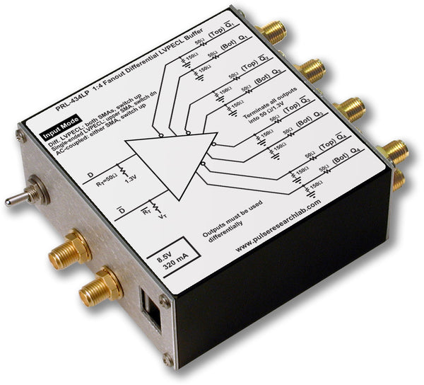
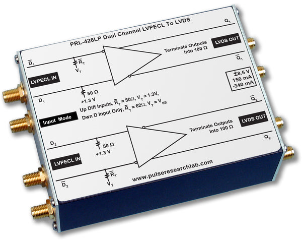
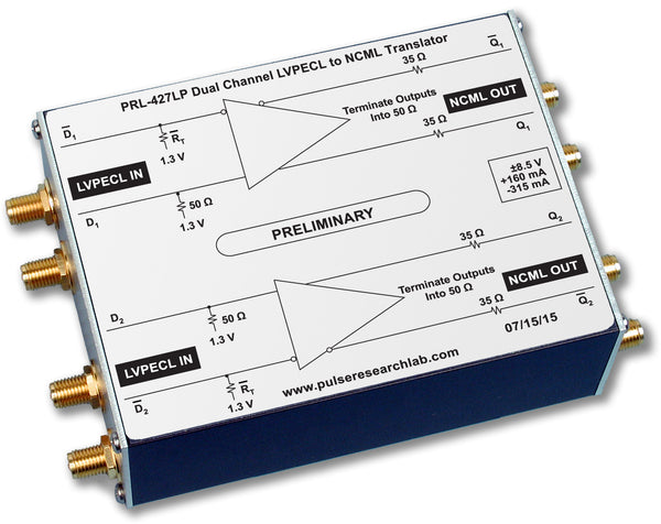
DescriptionThe PRL-424LV is a 1:4 fanout, complementary output, LVDS line driver. It has a floating 100 Ω universal differential input suitable for accepting LVDS, LVPECL, NECL, or RS-422 signals.(1) It also has a logically ORed, 50 Ω TTL input with a minimum 1 V triggering threshold. The PRL-424 high speed fanout line driver facilitates testing of high speed digital communications circuits and distribution of satellite signals. The floating differential input accepts differential LVDS, LVPECL, NECL, RS-422, or any 75 mV minimum differential signal within the window of -2 V to +3 V (option -01 has an input voltage range from -2.4 V to +4 V, and will accept 5 V PECL signals). When driven by LVPECL or NECL inputs, these signals must have internal 150 Ω or 200 Ω pull down resistors, respectively(1). The PRL-424 differential input is compatible with all LVPECL or NECL output signals from the PRL family of products. The connectors for the universal differential input are SMA, and the connector for the TTL input is BNC. All output connectors are SMA. The four pairs of complementary outputs are 50 Ω back-terminated and are designed for driving floating 100 Ω loads, normally the configuration used in LVDS input circuits. The output swing is typically 600 mV with a common mode voltage of 1.2 V. The PRL-424LV is supplied with a ±8.5 V/1.8 A AC/DC Adapter and housed in a 1.3 x 2.9 x 5-in. extruded aluminum enclosure. Available accessories include voltage distribution modules and brackets for mounting multiple units. (1) A related model, the PRL-424NLV, has a true NECL input terminated into 50 Ω/-2 V, and can accept single-ended or differential NECL signals that do not have internal pull-downs. |

(0° C ≤ TA ≤ 35° C)*
| SYMBOL | PARAMETER | Min | Typ | Max | UNIT | Comment |
|---|---|---|---|---|---|---|
| Rin | Differential Input Resistance | 99 | 100 | 101 | Ω | |
| RinC | Common Mode Input Resistance | 5k | Ω | |||
| Rout | Output Resistance | 49.5 | 50.0 | 50.5 | Ω | |
| VIN1 | Input Voltage Range | -2.0 | +3.0 | V | ||
| VIN2 | Option -01 Input Voltage Range | -2.4 | +4.0 | V | ||
| VOL | Output Low Level | 0.9 | V | |||
| VOH | Output High Level | 1.5 | V | |||
| VCMO | Output Common mode voltage1 | 1.2 | V | |||
| IDC1 | DC Input Current, +8.5 V | 130 | 140 | mA | ||
| IDC2 | DC Input Current, -8.5 V | -370 | -380 | mA | ||
| VDC | DC Input Voltage | ±7.5 | ±8.5 | ±12 | V | |
| VAC1 | AC/DC Adapter Input Voltage, 120 | 103 | 115 | 127 | V | |
| VAC2 | AC/DC Adapter Input Voltage, 220 | 206 | 220 | 254 | V | |
| tPLH | Propagation Delay to output ↑ | 2 | ns | |||
| tPHL | Propagation Delay to output ↓ | 2 | ns | |||
| tr/tf1 | Rise/Fall Times (10%-90%)2 | 500 | 650 | ps | @ 200 MHz | |
| tr/tf2 | Rise/Fall Times (10%-90%)2 | 250 | ps | @ 1.25 GHz | ||
| tSKEW | Skew between any 2 outputs | 200 | 550 | ps | ||
| fMAX1 | Max Clock Frequency, SMA Input3 | 1.25 | 1.35 | GHz | ||
| fMAX2 | Max Clock Frequency, TTL Input3 | 300 | MHz | |||
| Size | 1.3 x 2.9 x 5.0 | in. | ||||
| Weight | 8 | Oz | ||||
| Shipping Weight | 4 | lbs | ||||
Notes:
(1) VCMO = (VOH-VOL)/2
(2) Rise and Fall times measured with ground-referenced 50 Ω loads.
(3) fmax is measured using a PRL-425N with SMA input connectors as the receiver. The outputs of the PRL-425N are measured. fmax for the TTL input is currently limited by the lack of high frequency TTL divers.