Applications:
|
|
Features:
|
|
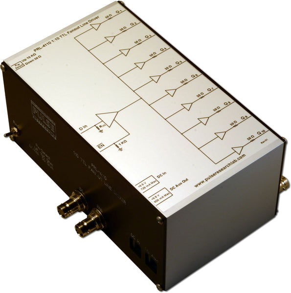
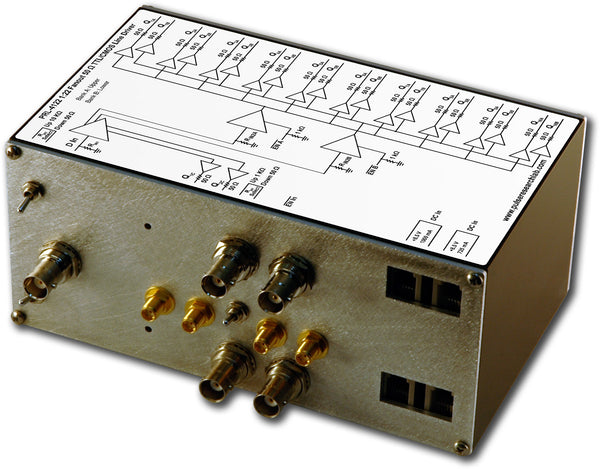
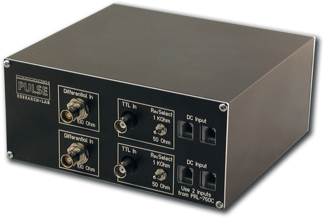
DescriptionThe PRL-4216UL-TR is a 2:16 fanout differential line driver module. Each bank has a pair of floating 100 Ω universal differential inputs suitable for accepting LVDS, LVPECL, NECL, or RS422 signals.(1) Each bank also has a a pair of logically ORed, 50 Ω TTL inputs with a minimum 1.0 V triggering threshold. Because the inputs are ORed a Hi level applied to either input can be used as a gate signal. Please see the block diagrams for more details. The 16 pairs of LVDS outputs are 50 Ω back-terminated and are designed for driving floating 100 Ω loads, normally the configuration used in LVDS input circuits. The output swing is typically 700 mV with a common mode voltage of 1.3 V. A PRL-4216UL-TR is equivalent in function to two of the PRL-4108UL-TR units housed in a single enclosure. Each internal PCB is independent. The PRL-4216UL-TR high speed fanout line driver facilitates testing of high speed digital communications circuits and distribution of satellite or telemetry signals. The floating differential input accepts differential LVDS, LVPECL, NECL, RS422, or any 75 mV minimum differential signal within a common-mode range of -2.0 V to +3.0 V. When driven by LVPECL or NECL inputs, these signals must have internal 150 Ω or 200 Ω pull down resistors, respectively (known as a "source-biased" output). The PRL-4216UL-TR differential input is compatible with all LVPECL or NECL output signals from the PRL family of products. The TTL input has a selectable 50 Ω/1 kΩ input load and will trigger on a minimum 1.0 V threshold. The 1 kΩ is useful for interfacing with low-power circuits. The PRL-4216UL-TR is supplied with a ±8.5 V/1.8 A AC/DC Adapter and housed in a 3.0 x 6.8 x 6.0-in. extruded aluminum enclosure. Available accessories include voltage distribution modules and mating cables. (1) A related series, the PRL-4216NL, has a true NECL input terminated into 50 Ω/-2 V, and can accept single-ended or differential NECL signals that do not have internal pull-downs. |
 Fig. 1: PRL-4216UL-TR Simplified Block Diagram, One of Two Identical PCBs Shown
(0° C ≤ TA ≤ 35° C)*
Unless otherwise specified, dynamic measurements are made with all rear-panel outputs terminated into floating 124 Ω, using 124 Ω shielded twisted pair Triax cables (Trompeter P/N PCGOW10PCG-36 or equivalent). Channel to channel skew and propagation delay measurements are made using a PRL-425NTR Differential Receiver with NECL outputs. Rise and fall time measurements are made using a Triax to SMA adapter and connecting the SMA outputs to a 50 Ω input scope.
| Symbol | Parameter | Min | Typ | Max | Unit | Comments |
|---|---|---|---|---|---|---|
| RT1-1 | Differential Input Resistance | 95 | 100 | 105 | Ω | |
| RINC | Common Mode Input Resistance | 5 | kΩ | |||
| RT2-1 | Input Resistance, TTL 50 Ω | 49 | 50 | 51 | Ω | |
| RT2-2 | Input Resistance, TTL 1 kΩ | 0.95 | 1.00 | 1.05 | kΩ | |
| VCMR | Input Common Mode Voltage | -2.0 | 3.0 | V | ||
| VIH1 | TTL Input Hi Level | 1.0 | 5.0 | V | Internally limited to 3.5V | |
| VIL1 | TTL Input Lo Level | -0.5 | 0.5 | V | ||
| ROUT1 | Output Resistance | 24.75 | 25 | 25.25 | Ω | Single-ended |
| ROUT2 | Output Resistance | 49.5 | 50 | 50.5 | Ω | Differential |
| VOH1 | Output High Level | 1.8 | V | No Load | ||
| VOH2 | Output High Level | 1.65 | V | Terminated to 100 Ω | ||
| VOL1 | Output Low Level | 0.78 | V | No Load | ||
| VOL2 | Output Low Level | 0.95 | V | Terminated to 100 Ω | ||
| VOD | Output Differential Voltage (VOH2-VOL2) | 0.7 | Terminated to 100 Ω | |||
| VOCM | Output Common Mode Voltage* | 1.3 | Terminated to 100 Ω | |||
| VAC1 | AC Adapter Input Voltage, 120 V | 108 | 115 | 127 | V | |
| VAC2 | AC Adapter Input Voltage, 220 V | 216 | 230 | 254 | V | |
| IDC1 | DC Input Current, +8.5 V Supply | 770 | mA | |||
| IDC2 | DC Input Current, -8.5 V Supply | -1400 | mA | |||
| TPROP1 | Prop. Delay to Output ↑, Diff. Input | 2.5 | ns | |||
| TPROP2 | Prop. Delay to Output ↑, TTL Input, 50 Ω | 3 | ns | |||
| TR | Rise Time (10%-90%) | 1.2 | 1.8 | ns | See Note 1 | |
| TF | Fall Time (10%-90%) | 1.2 | 1.8 | ns | See Note 1 | |
| TSKEW1 | Ch./Ch. skew ↔ any 2 ↑ or 2 ↓VO in each bank | 200 | 350 | ps | ||
| TSKEW2 | Ch./Ch. skew ↔ any ↑ and ↓VO in each bank | 700 | 1200 | ps | ||
| TSKEW3 | Ch./Ch. skew ↔ any 2 ↑ or 2 ↓VO | 400 | 550 | ps | ||
| TSKEW4 | Ch./Ch. skew ↔ any ↑ and ↓VO | 1000 | 1250 | ps | ||
| FMAX1 | Max Clock Frequency, Diff. Input | 150 | 175 | MHz | ||
| FMAX2 | Max Clock Frequency, TTL Input | 100 | 125 | MHz | ||
| Size | 3.0”H x 6.8”W x 7.3”L | in | Including connectors | |||
| Weight | 2 | lbs | Excluding AC adapter | |||
| Shipping weight | 6 | lbs | Including AC adapter | |||