NECL/PECL FAQs
- Q0: How do I distribute and translate NECL/PECL/LVPECL signals?
- Q1: What are ECL Circuits?
- Q2: What are the ECL supply voltages?
- Q3: What are LVECL, PECL and LVPECL Devices?
- Q4: What are the Logic Levels for ECL, LVECL, PECL and LVPECL Circuits?
- Q5: What does a typical ECL input circuit look like?
- Q6: What does a typical ECL output circuit look like?
- Q7: How do I drive ECL Inputs connected to 50 Ω/VTT Terminations?
- Q8: How do I drive a floating Differential ECL Input?
- Q9: Why do ECL signals need to be terminated, and where do I get this 50 Ω/-2 V termination?
- Q10: What are Reflections, and how do I get rid of them?
- Q11: Can a Differential Input ECL device be used as a Voltage Comparator?
- Q12: How do I drive an AC coupled 50 Ω load with an ECL output?
- Q13: What happens if I overdrive an ECL Input?
- Q14: Why can’t I measure any output from an ECL output connector? How should I measure it?
- Q15: What happens if I short an ECL or PECL output to ground?
- Q16: How do I tap into an ECL I/O line to look at the signal?
Q0: How do I distribute and translate NECL/PECL/LVPECL signals?
A0: Pulse Research Lab offers a wide variety of products for handling ECL signals:
- Fanout buffers for NECL signals or LVPECL signals.
- Translating from NECL signals, PECL signals, or LVPECL signals
- Translating to NECL signals, PECL signals, or LVPECL signals
- Re-buffering NECL and LVPECL signals for driving long lines
- Our most popular ECL products are:
- PRL-420ND, 2 Channel TTL to Differential NECL Translator
- PRL-450ND, 2 Channel Differential NECL to TTL Translator
- PRL-434A, 1:4 Differential NECL Fanout Buffer
- PRL-431AN-SMA, 1:2 Differential NECL Fanout Buffer
- PRL-434LP, 1:4 Differential NECL Fanout Buffer
- PRL-430AN-SMA, 2 Channel Differential NECL Line Driver
A1: ECL stands for Emitter Coupled Logic. The basic circuit configuration consists of a pair of NPN transistors with their emitters connected together and fed by a current source as show in Fig. 1.
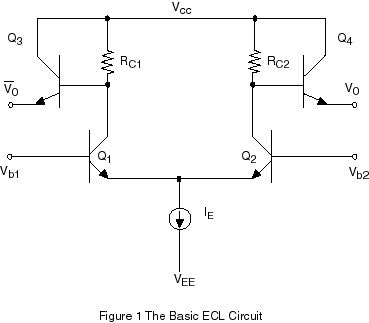
Q1 and Q2 are normally referred to as the differential switch. In the steady state, either Q1 or Q2 is on but not both, and the output logic state is determined by the voltage difference between the bases of Q1 and Q2. If Vb1 – Vb2 > 200 mV, Q1 will be turned on and Q2 turned off, and vice versa.
The inputs can be driven either differentially or single-ended. In the single-ended mode, the non-driven base must be connected to a suitable bias voltage, VBB, which is either supplied internally by the device, or externally. The voltages developed at the collectors of Q1 and Q2 are connected to a pair of emitter followers, Q3 and Q4. The outputs are taken at the emitters of Q3 and Q4. Note that the output emitters are open, and, unlike TTL/CMOS circuits, there will be no output until a pull-down resistor is connected to the open emitter. This pull-down resistor plays a very important role in determining the performance of the ECL circuit, (see other FAQs). A more detailed description of the basic ECL circuits and the variation of circuit configurations can be found in the Motorola MECL Data book and the newer High Performance ECL Data book.
Q2: What are the ECL Supply Voltages?
A2: There are normally two supply voltages specified. The more positive supply voltage is labeled VCC and the more negative supply voltage VEE. Usually, only one supply voltage is used, and the other is ground. One may also see ECL evaluation boards with both positive and negative voltages used in order to simplify interfacing with ground-referenced instruments.
In the newer ECLinPS and ECLinPS Lite families of GHz ECL devices, both 10 K and 100 K devices can share the same supply voltages of VCC-VEE = -5.2 V. The industrial standard for ECL supply voltages are VCC=0 V, and VEE = -5.2 V.
Q3: What are LVECL, PECL and LVPECL Circuits?
A3: LVECL devices are ECL devices designed for use with VEE = -3.3 V. They are I/O compatible with standard ECL devices.
The "P" in PECL stands for positive. PECL Circuits are generally identical to ECL circuits, except the VCC supply is 5 V and the VEE supply is ground. There are special PECL devices that are designed strictly for +5 V supply only.
LVPECL Circuits are PECL circuits designed for use with VCC = 3 V or 3.3 V, the same supply voltage as for Low Voltage CMOS devices. As one can see, the PECL and LVPECL devices are designed to be supply voltage compatible with TTL/CMOS and LVCMOS circuits, respectively.
Q4: What are the Logic Levels for ECL, LVECL, PECL and LVPECL Circuits?
A4: For the sake of simplicity, only nominal values will be used for the discussion here. Worst case values as a function of loading, temperature and supply voltage variations can be found in the Motorola Data Book.
For standard ECL circuits, the Hi and Lo logic levels are defined to be VCC-0.8 V and VCC-1.6 V, respectively. Since these levels are referenced to the VCC supply only, they are applicable to ECL’s, LVECL’s, PECL’s and LVPECL’s. The following table lists the nominal numerical values of logic levels for these circuits, including the internal bias voltage VBB and the external termination voltage VTT, which must be supplied by the user.
When driving these devices using a 50 Ω-output generator, the output Hi and Lo levels of the generator must be set so that the correct levels are produced at the input of these devices. For a device with input terminated to 50 Ω/VTT, the resistor divider effect between the generator source resistance and the load must be taken into account, and the equivalent circuit is shown in Fig. 5.
From Fig. 5, the required open circuit Hi and Lo levels from the 50 Ω-output generator are easily calculated and are listed below as VOHPG and VOLPG.
| ECL | LVECL | PECL | LVPECL | |
| VCC | 0 V | 0 V | +5.0 V | +3.3 V |
| VEE | -5.2 V | -3.3 V | 0 V | 0 V |
| VOH | -0.8 V | -0.8 V | +4.2 V | +2.5 V |
| VOL | -1.6 V | -1.6 V | +3.4 V | +1.7 V |
| VBB | -1.3 V | -1.3 V | +3.7 V | +2.0 V |
| VTT | -2 V | -2 V | +3 V | +1.3 V |
| VOHPG | +0.4 V | +0.4 V | +5.4 V | +3.7 V |
| VOLPG | -1.2 V | -1.2 V | +3.8 V | +2.1 V |
Table I: I/O and Bias voltage levels for ECL, LVECL, PECL and LVPECL devices
It is important to note that the I/O levels, VBB and VTT for both ECL and LVECL are the same but not so for PECL and LVPECL devices. It should be pointed out that these logic levels are affected some what by the loading conditions. For ECL’s, for example, under heavy loading conditions, VOH may be –0.95 V instead of –0.8 V. Similarly, VOL may be –1.75 V instead of –1.6 V. For convenience sake, the VOLPG values can be chosen to be the same as the VTT values, resulting, in slightly different propagation delays between the output rising and falling edges, because the input waveform is no longer symmetrical with respect to VBB.
Q5: What does a typical ECL input circuit look like?
A5: Instead of describing each ECL, LVECL, PECL or LVPECL input circuit separately, we shall focus on the generalized "ECL" circuit, with a VCC supply and a VEE supply.
The basic input circuit of an ECL device is simply the base of a NPN transistor. For a device installed inside a piece of equipment, however, some form of an input termination is always used. The most common input configuration is one that has a 50 Ω termination into VTT, where VTT is defined as VCC- 2 V. This configuration is used for either single-ended or differential inputs, as shown in Fig. 2A.

The second configuration consists of a single floating resistor connected between the differential inputs of an ECL device, as shown in Fig. 2B.

The most common value of this resistor is 124 Ω. Other values such as 75 Ω, 78 Ω, and 100 Ω are also used. The third consists of two resistors in series, and the series combination is connected across the differential inputs of the ECL device, and the junction of the resistors is bypassed by a capacitor to ground, as shown in Fig. 2C. Other configurations are also used.
The reason why ECL input circuits inside a piece of equipment must always be terminated as described above has to do with matching impedance. Without proper input terminations, it would not be possible to interconnect various equipment together.
Q6: What does a typical ECL Output Circuit look like?
A6: As shown in Fig. 1 earlier, the ECL output circuit consists of an open NPN emitter, and it was also pointed out that a pull-down resistor is needed in order to turn on the emitter follower. In a piece of equipment provided with ECL outputs, however, internal pull-down resistors may or may not be included. Since pull-down resistors consume power, the equipment manufacturers don’t put them in unless they have to. If it is not labeled, it may be assumed that they are not included. As we shall see in the following discussion (Question 7), ECL outputs without the proper internal pull-down resistors cannot drive AC coupled loads or floating loads.
Q7: How to Drive ECL Inputs connected to 50 Ω/VTT Terminations?
A7: There are two cases to consider. The first involves using an ECL output device as the driver, and the second uses a 50 Ω output generator. In the first case, there is nothing to adjust, and the question is whether or not the I/O are compatible. In the second case, the generator output Hi and Lo levels must be adjusted so that they produce the correct levels at the input of the receiving device. In the following discussion, the standard ECL levels will be used. The basic principle is applicable to LVECL, PECL and LVPECL as well.
Case I: The driver is an ECL device.
For a single input configuration, it can be connected directly to the open emitter of an ECL output connector via a 50 Ω cable, as shown in Fig. 3.

It is seen that the 50 Ω resistor connected to –2 V supplies the current to the open emitter, and, therefore, no pull-down resistor is needed from the driver emitter follower. Note that the unused input is assumed to be connected to a bias voltage VBBinternally as shown. If a pair of differential input connectors are present, either the unused input must be connected to VBBexternally or both inputs must be driven using a pair of complementary signals.
Although no calculation is required for interconnecting the I/O’s in this case, the simple calculation given below is helpful in seeing why the pull-down resistor plays an important part. Assuming the "hi" and "lo" logic levels developed under this "heavy loading" condition to be –0.95 V and –1.75 V, respectively, the output currents from the driver circuit can be easily calculated to be:
IOH=(2-0.95)V/50 Ω =21 mA and
IOL=(2-1.75)V/50 Ω =5 mA
The exact values of the currents are not important, as long as they are positive numbers, because an NPN emitter can only source current but not sink current. An ECL output with internal pull-down resistor can also drive this type of input circuit. It should be noted that a 50 Ω cable must be used for this configuration because the load at the end of the cable is 50 Ω. For more discussion see Transmission Line FAQs.
Case II: The driver is a 50 Ω-output Generator
Fig. 5 shows an equivalent circuit of a 50 Ω-output pulse generator connected to a 50 Ω/-2 V input terminated ECL circuit.

In order to produce a set of Hi and Lo levels equal to -0.8 V and –1.6 V, respectively, at the ECL device input, the open circuit Hi and Lo levels of the pulse generator should be set to +0.4 V and –1.2 V, respectively. This is easily verified by calculating the current in each logic state using Fig. 5. Often, for convenience, the Lo level of –2 V is used. However, the –0.8 V/-2 V levels are not symmetrical with respect to the ECL threshold voltage VBB, which has a typical value of –1.3 V. The net result of using this set of input voltages is that the propagation delays of the output rising and falling edges will not be exactly the same.
The output levels of the 50 Ω-output Generator required for LVECL, PECL and LVPECL are given in A4, Table I. It is important to note that ECL and LVECL are compatible, but PECL and LVPECL are not.
Q8: How to Drive a Floating Differential ECL Input?
A8:
Case I: The drivers are a pair of differential ECL devices.
This type of input circuit can be represented by the configuration shown in Fig. 2B or 2C. Because it has an equivalent floating resistor, no current path exists for the driver open NPN emitters. Therefore, only differential output circuits with the "appropriate" pull-down resistors can drive this type of load. A pair of 300 Ω pull-down resistors can handle either 124 Ω or 75 Ω floating input.
|
|
|
Next, let's see what we mean by "appropriate." Let's take the input configuration shown in Fig. 2B and connect it to a pair of differential output emitter followers including pull-down resistors, R5 and R6, as shown in Fig. 4. Lets assume the "hi" and "lo" logic levels to be –0.8 V and –1.6 V, respectively, a lightly loaded condition. The difference of these voltages, which is the logic swing of 0.8 V, appears across the 124 Ω resistor, resulting in a current flow of 6.45 mA. This current must be sourced by the emitter follower in the "hi" state and sunk by the emitter follower in the "lo" state.

Knowing this, we can easily calculate the appropriate value for R5 and R6. As we mentioned above, the NPN emitter cannot sink current. Therefore, the current in the pull-down resistor, say R6, in the "lo" state must be made larger than 6.45 mA; otherwise, the emitter follower will be cut off before it reached the intended "lo" state. This requirement sets the condition that
(5.2 V-1.6 V)/R6 = 6.45 mA.
Solving for R6, it is seen that it must be less than 558 Ω. In another words, unless the output emitter followers have internal pull-down resistors with values less than 558 Ω, the drivers cannot drive this differential load properly. Chances are that the circuit will still work if the resistor value is higher than 558 Ω, but the frequency response and noise margin will suffer, because the "lo" level will not attain its full value of –1.6 V.
Now let's look at the configuration in Fig. 2C; the resistors are assumed to be each 50 Ω. It is easily seen that this is almost identical to the case just described. The pull-down resistors need to be less then 450 Ω instead.

The next logical question to be asked is "What does one do if the ECL outputs are not provided with pull-down resistors and the load is a differential floating resistor?" One option is to add pull-down resistors at the output emitter followers, if one has access to the circuit. If not, then an ECL buffer circuit with a 50 Ω/-2 V input terminations and differential outputs with 200 Ω pull-down resistors would be needed( See PRL-430A data sheet ). Adding Pull-down resistors somewhere in between the open emitter outputs and the floating resistor input should be avoided, because this would cause an impedance mismatch.
As discussed in the first example, a cable with a Characteristic Impedance matching the load termination must also be used. For this example, a 124 Ω shielded twisted pair with the proper connectors would be required.
Case II: The Drivers are the complementary outputs from a 50 Ω-output generator.
Since the floating resistor in a differential input configuration is not necessarily 50 Ω, one would need to use the equivalent circuit shown in Fig.6 to determine the proper pulse generator output level setting.

For example, let's assume the floating load resistor RL is 124 Ω. If the pulse generator open circuit output Hi and Lo levels are assumed to be E1 and E2, respectively, then the required voltage at V1 and V2 are, respectively –0.8 V and –1.6 V. This translates to a current flow of 6.45 mA through all three resistors. Working backwards, E1 should be set to –0.8 V + 6.45 mA x 0.05 kΩ =-0.478 V and E2 should be set to –1.6 V- 6.45 mA x 0.05 kΩ = -1.92 V.
In this differential input configuration, the interconnecting cable can be either 50 Ω or 124 Ω depending on the choice of the interfacing connector arrangement. If a twinax or triax connector is used in the differential input end, then a 50 Ω input to 124 Ω differential output converter, such as the PRL-433, together with a 124 Ω cable can greatly simplify the interface. If the differential input uses two SMA or BNC connectors, then 50 Ω cables should be used. In either case, there is impedance match in one direction only, a topic to be posted later on the web.
Q9: Why do ECL Signals need to be terminated and where do I get this 50 Ω/-2 V Termination?
A9: ECL signals have very fast transition times. For devices in the 10KH and 100KH series, the output transition times are in the 1.5 to 2 ns range. For devices in the 10EP/100EP series, however, transition times can be in the 150-250 ps range. When dealing with transmission of signals having these short transition times, terminating the signal into the Characteristic Impedance, Zo, of the interconnecting device is mandatory, not an option. For coaxial cables, common values for Zo are 50 Ω, 75 Ω, and 93 Ω. Other Zo values such as 78 Ω and 124 Ω are available in shielded twisted cables.
The general theory is that when the transition time of the signal is "short" compared to the interconnect propagation delay, then a "long line", or transmission line, environment exists, and transmission line treatment of the circuit must be used. Typical propagation delay of a 50 Ω cable, such as the RG178, is 1.65 ns/ft. A short discussion providing an intuitive picture of what the transmission line effect is all about will soon be available via our FAQ section under the category "Transmission Line".
There is no hard and fast rule which separates a "short line" from a "long line," although numbers from 2 to 5 for the ratio of the interconnect delay to the signal transition time have been suggested for the definition of a "long line". More discussion on this subject can be found in Motorola MECL Systems Design Handbook and in a number of GaAs device data books. Rigorous treatments of the transmission theory can be found in the classical text book, Walter C. Johnson, "Transmission Lines and Networks", McGraw-Hill, 1950, Part I, Chapters 1-9.
Q10: What are reflections and how do I get rid of them?
A10: Reflections are energies not absorbed at the load that must be returned or reflected back to the source. There will be no reflection when the load impedance is equal to the Characteristic Impedance Zo of the transmission media.
Q11: Can a Differential Input ECL device be used as a Voltage Comparator?
A11: Yes. Many devices in the newer ECLinPS and ECLinPS Lite families have a typical common mode range of VCC–0.4 V maximum to VEE +2.5 V minimum. This relatively wide common mode range enables a differential input ECL receiver device, shown in Fig. 2A, 2B or 2C to be used as a comparator.
|
|
|
|
Either input in Fig. 2A can also be driven by a single-ended AC coupled sine or square wave signal, because such a signal would swing symmetrically with respect to the non-driven input which is now biased at VTT.
In fact, the PRL-430A Differential ECL Receiver is used as a receiver/comparator for detecting weak signals in a number of satellite communications systems. The complementary outputs of the PRL-430 are suitable for driving up to 200 feet of 50 Ω cables.
Q12: Can an ECL Output Drive an AC coupled 50 Ω load?
A12: When driving an AC coupled 50 Ω load, the ECL output emitter follower must obtain its DC supply current from the pull-down resistor. If the logic swing is to be maintained at 800 mV, the discharge current flowing out of the 50 Ω load resistor during the downward swing of the signal must be equal to (0.8 V/50 Ω)=16 mA, and this current flows into the output NPN emitter, as shown in Fig. 7.
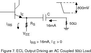
Since the NPN emitter can only source current, the current in the pull-down resistor must be made larger then 16 mA so that the emitter current IE is always positive. Assuming that the "lo" state output emitter voltage is –1.6 V, the maximum value of the pull-down resistor is calculated to be equal to (5.2 V-1.6 V)/16 mA=225 Ω. Typically, a 200 Ω pull-down resistor is used when AC coupling to a 50 Ω load is required.
For power consumption reasons, most equipment with ECL outputs do not include internal pull-down resistors. A 200 Ω pull-down resistor draws an average current of 20 mA. In a system where 64 output drivers are required, for example, this translates to an additional current drain of 1.28 A if every output has a 200 Ω pull-down resistor.
Q13: What happens if I Over Drive an ECL Input?
A13: If one refers back to Fig. 1, the collector voltage of the "on" transistor Q1 is VCC-0.8 V.
If the base of Q1 is raised above VCC - 0.2 V, the base to collector diode of Q1 will be forward biased, resulting in increased turn off delay of Q1. Excessive overdrive applied to any ECL input above VCC or below VEE can damage the device.
Q14: Why can’t I get any output from an ECL Output Connector, and how should I measure it?
A14: In Fig. 1 above, it was shown that ECL outputs are open emitters. Without pull-down resistors, the outputs are turned off and therefore, there is no output voltage. Even if the output has an internal pull-down resistor, it may still not be possible to measure the true output signal either, unless the measurement device is impedance-matched to the ECL output structure. The reason for this problem is that the internal connection between the output ECL device pin and the output connector is most likely a "long line," and neither the scope probe nor the high impedance scope input represents an impedance match to the ECL output structure.
If one was to connect the ECL output directly to the 50 Ω oscilloscope input, there would no output either, because the output emitter will be turned off by the ground-referenced 50 Ω input, even if the output has a 200 Ω pull-down resistor. However, AC coupling an ECL output with an internal 200 Ω pull-down resistor to a 50 Ω input instrument is OK (See Question 12).
So much for not being able to measure an ECL signal, now we shall show how it can be measured using an ECL Terminator.
ECL/PECL output circuits are designed to drive 50 Ω loads terminated into a terminating voltage VTT= VCC-2 V. For ECL, VCC = 0 V, and VTT = -2 V. For PECL, VTT = +3 V. If the input of a measurement instrument is made to look just like a 50 Ω/VTT termination, then all should be well. In fact, that is exactly what an ECL or PECL Terminator is.
An ECL Terminator is basically a biased 50 Ω microwave attenuator. The input has an equivalent 50 Ω/-2 V terminatation, and the output is suitable for driving a ground referenced 50 Ω input instrument. Similarly, the input of a PECL Terminator has an equivalent 50 Ω/3 V termination. In order to protect sensitive instruments, however, a properly designed ECL/PECL terminator should have a near ground level output (See the PRL-550NQ4X data sheet).
For measuring a differential ECL output using a Twinax or Triax connector, either an instrument with a differential input and the proper termination or a differential to single-ended converter is required.
Caution! Do not connect the output of a PECL device to an ECL terminator or to a ground-referenced 50 Ω input instrument. This could spell instant disaster for the PECL device or the instrument (See Question 15). Although connecting an ECL output to a PECL Terminator may not destroy the ECL device, it could cause gradual degradation of the output emitter follower, due to possible excessive reverse bias voltage developed across the base to emitter junction.
Q15: What happens if I short an ECL or PECL Output to Ground?
A15: In Fig. 1 above, it is shown that the collectors of the ECL output emitter followers are connected to VCC. When VCC is ground, shorting the emitter to ground merely turns off the emitter follower and no damage will occur.
This is not the case when VCC is = +5 V. The transistor output current is limited only by b times its base current, which is supplied by R1 or R2 connected to VCC. In most cases, the device is destroyed instantly. In fact, connecting a PECL output device to a ground-referenced 50 Ω load often destroys the device instantly as well.
Q16: How do I tap into an ECL I/O Line to look at the signal?
A16: As discussed in Question 9, fast ECL signals need to have their I/O lines terminated. A 10X coaxial probe, as shown in Fig. 8, allows the extraction of a part of the signal for measurement and still maintains the impedance match at the I/O ports.

The 10X coaxial probe splits a signal into a 90% amplitude output and a 10% amplitude, or 10X, output, which can be connected to the 50 Ω input of an oscilloscope. This 10X coaxial probe is designed for use in a 50 Ω environment, where every port is to be terminated into 50 Ω . When properly terminated, it has the property that the input impedance of the signal input port and the output impedance of the 90% signal output port are both 50 Ω .
Although the output resistance of an ECL device is not 50 Ω, the input port of the 10X probe does look into a 50 Ω impedance when the other two ports are terminated into 50 Ω. Therefore, when an ECL output circuit is connected to the input port of this probe, it sees a 50 Ω impedance when the other two ports are terminated into 50 Ω/-2 V and 50 Ω, respectively. This satisfies the condition that the ECL output is properly terminated.
This probe arrangement works quite well with either a single-ended ECL or PECL signal, although the 10% signal loss in the through path may be of concern as it reduces the noise margin of the signal as well. However, by using a dual channel probe, such as the PRL-860D, for transmitting both the true and complement output signals, the noise margin will be improved.